
- English
- Español
- Português
- русский
- Français
- 日本語
- Deutsch
- tiếng Việt
- Italiano
- Nederlands
- ภาษาไทย
- Polski
- 한국어
- Svenska
- magyar
- Malay
- বাংলা ভাষার
- Dansk
- Suomi
- हिन्दी
- Pilipino
- Türkçe
- Gaeilge
- العربية
- Indonesia
- Norsk
- تمل
- český
- ελληνικά
- український
- Javanese
- فارسی
- தமிழ்
- తెలుగు
- नेपाली
- Burmese
- български
- ລາວ
- Latine
- Қазақша
- Euskal
- Azərbaycan
- Slovenský jazyk
- Македонски
- Lietuvos
- Eesti Keel
- Română
- Slovenski
- मराठी
- Srpski језик
China CVD sic Hersteller, Lieferanten, Fabrik
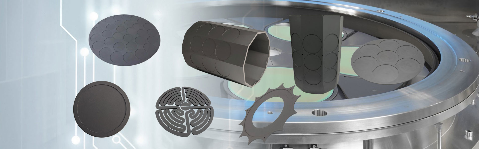
CVD SiC is a vacuum deposition process used to produce high-purity solid materials. This process is often used in semiconductor manufacturing to form thin films on wafer surfaces. During the chemical vapor deposition (CVD) process for producing silicon carbide (SiC), a substrate is exposed to one or more volatile precursors, which chemically react on the substrate surface to form the desired SiC deposit. Among the various methods for producing SiC, CVD produces products with high uniformity and purity, and offers strong process controllability.
Simply put, CVD SiC refers to SiC produced via the chemical vapor deposition (CVD) process. In this process, gaseous precursors, typically containing silicon and carbon, react in a high-temperature reactor to deposit a thin SiC film onto a substrate. CVD SiC is valued for its exceptional properties, including high thermal conductivity, chemical inertness, mechanical strength, and resistance to thermal shock and wear. These properties make chemical vapor deposited (CVD) silicon carbide (SiC) ideal for demanding applications such as semiconductor manufacturing, aerospace components, armor, and high-performance coatings. This material's exceptional durability and stability under extreme conditions ensure its effectiveness in improving the performance and lifespan of advanced technologies and industrial systems.
CVD SiC materials, due to their unique combination of excellent thermal, electrical, and chemical properties, are well-suited for applications in the semiconductor industry, where high-performance materials are required. Chemical vapor deposited (CVD) silicon carbide (SiC) components are widely used in etching equipment, MOCVD equipment, Si and SiC epitaxy equipment, and rapid thermal processing equipment.
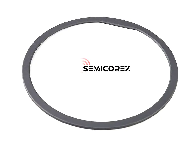
The largest market segment for CVD SiC components is etching equipment components. Due to its low reactivity to chlorine- and fluorine-containing etching gases and its electrical conductivity, CVD silicon carbide (SiC) is an ideal material for components such as focus rings in plasma etching equipment. CVD silicon carbide (SiC) components in etching equipment include focus rings, gas showerheads, trays, edge rings.
Take the focus ring, for example. This critical component is placed outside the wafer and in direct contact with it. Voltage is applied to the ring to focus the plasma passing through it, thereby focusing the plasma on the wafer and improving processing uniformity. Traditionally, focus rings are made of silicon or quartz. However, with the advancement of integrated circuit miniaturization, the demand for and importance of etching processes in integrated circuit manufacturing continues to increase. The power and energy of the plasma used for etching are also increasing, especially in capacitively coupled plasma (CCP) etching equipment, which requires even higher plasma energies. Consequently, focus rings made of silicon carbide are becoming increasingly popular.
Due to the high performance of CVD SiC and its ability to be sliced into very thin sections, it can also benefit sputter targets and all types of electrodes.
Process of Chemical Vapor Deposition (CVD)
CVD is a process that transforms a material from a gas phase to a solid phase, used to form a thin film or coating on a substrate surface. The following are the basic steps in CVD:
1. Substrate Preparation
Choose an appropriate substrate material and perform the appropriate cleaning and surface treating to produce a clean, flat surface with good adhesion.
2. Reactive Gas Preparation
Prepare the necessary amount of reactive gas or vapor and inject it into the deposition chamber by some means (gas supply system). The reactive gas can be an organic compound, a metal-organic precursor, inert gas, or other gaseous species.
3. Deposition Reaction
If all instrumentation is setup correctly the CVD process will begin under the pre-defined reaction conditions. The reactive gas that has been injected into the chamber will undergo some chemical or physical reaction on the substrate surface to form a deposit onto the substrate surface. The deposit formation can be the result of several types of processes depending on the deposition method, these include vapor-phase thermal decomposition, chemical reaction, sputtering, epitaxial growth, etc.
4. Control and Monitoring
At the same time during the deposition process, certain deposition parameters need to be controlled and monitored in real time if the observer wishes to ensure the best possible properties in the film are maintained. These include relevant temperature measurement, pressure monitoring, and regulation of gas flow, all the while aiming to keep the desired reaction conditions stable and constant.
5. Deposition Completion and Post-Processing
When either the deposition time, predetermined thickness, or method selected, is achieved the introduction of the reaction gas can be ceased and deposition process ended. Following the deposition, several pertinent post-processing methods (annealing, structural modifications, surface treatment, etc.) should be performed to improve the film performance/quality.
It's important to note that the specific vapor deposition process can vary depending on the deposition technology, material type, and application requirements. However, the basic process outlined above covers most common vapor deposition steps.


- View as
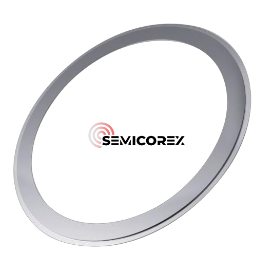
Erdungsring der oberen Elektrode
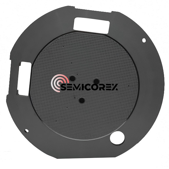
Der Erdungsring für die obere Elektrode von Semicorex ist eine hochreine CVD-SiC-Plasmakontrollkomponente, die das elektrische Potenzial stabilisiert und eine gleichmäßige Plasmaverteilung in fortschrittlichen Halbleiterätz- und -abscheidungssystemen unterstützt. Semicorex liefert weltweit Präzisions-CVD-SiC-Erdungsringe und plasmabeschichtete Halbleiterkomponenten und bietet maßgeschneiderte Abmessungen, elektrische Eigenschaften und zuverlässige globale Lieferung für führende Hersteller von Halbleiterausrüstungen.*
WeiterlesenAnfrage absenden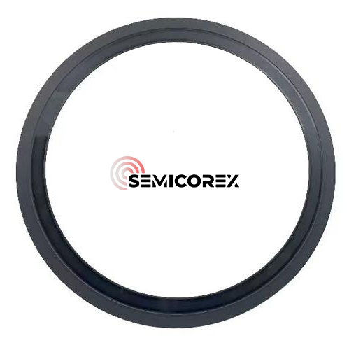
Ätzkantenring
Der Semicorex Etching Edge Ring ist eine hochreine CVD-SiC-Plasmakomponente, die die Plasmaverteilung um die Waferkante steuert und so die Gleichmäßigkeit der Ätzung, die Prozessgenauigkeit und die Gesamtleistung bei der Halbleiterfertigung verbessert. Semicorex beliefert Halbleiterhersteller auf der ganzen Welt mit fortschrittlichen CVD-SiC-Fokusringen, Erdungsringen, Duschköpfen und maßgeschneiderten Plasmakontrollkomponenten, unterstützt durch Präzisionstechnik und zuverlässige globale Lieferung.*
WeiterlesenAnfrage absenden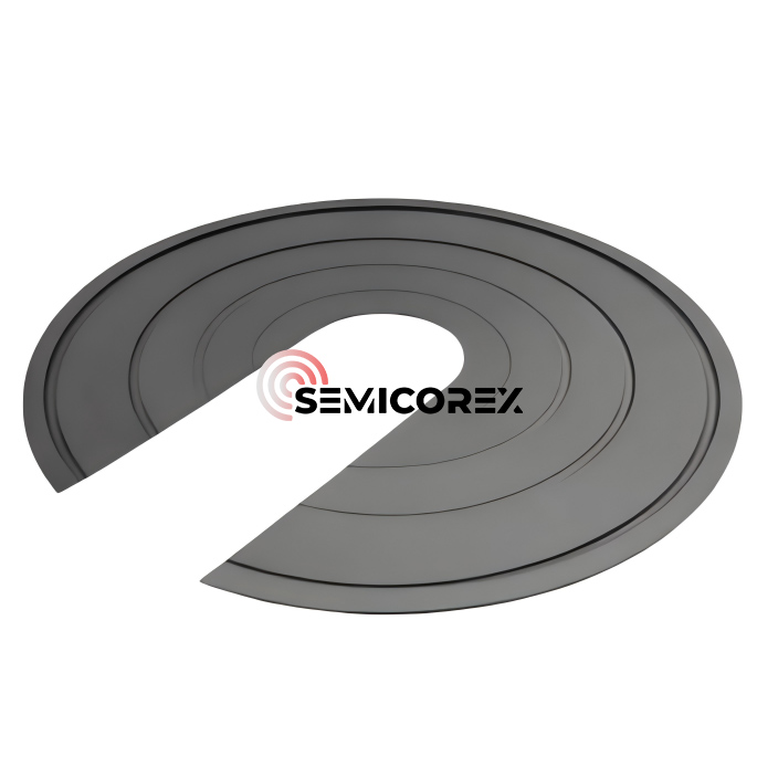
CVD-SiC-Fin
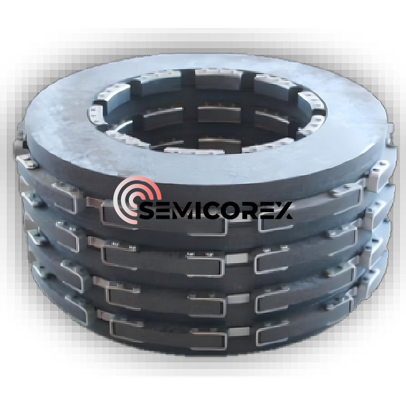
Semicorex CVD SiC Fin ist eine dicke, hochdichte feste Siliziumkarbidkomponente, die durch chemische Gasphasenabscheidung hergestellt wird und für Plasma- und Ultrahochtemperatur-Halbleiteranwendungen entwickelt wurde, die außergewöhnliche Reinheit, Haltbarkeit und Korrosionsbeständigkeit erfordern. Semicorex liefert fortschrittliche CVD-Siliziumkarbid-Komponenten an Hersteller von Halbleiterausrüstungen weltweit und bietet maßgeschneiderte Lösungen, Präzisionstechnik und zuverlässige globale Lieferung für die anspruchsvollsten Prozessumgebungen.*
WeiterlesenAnfrage absenden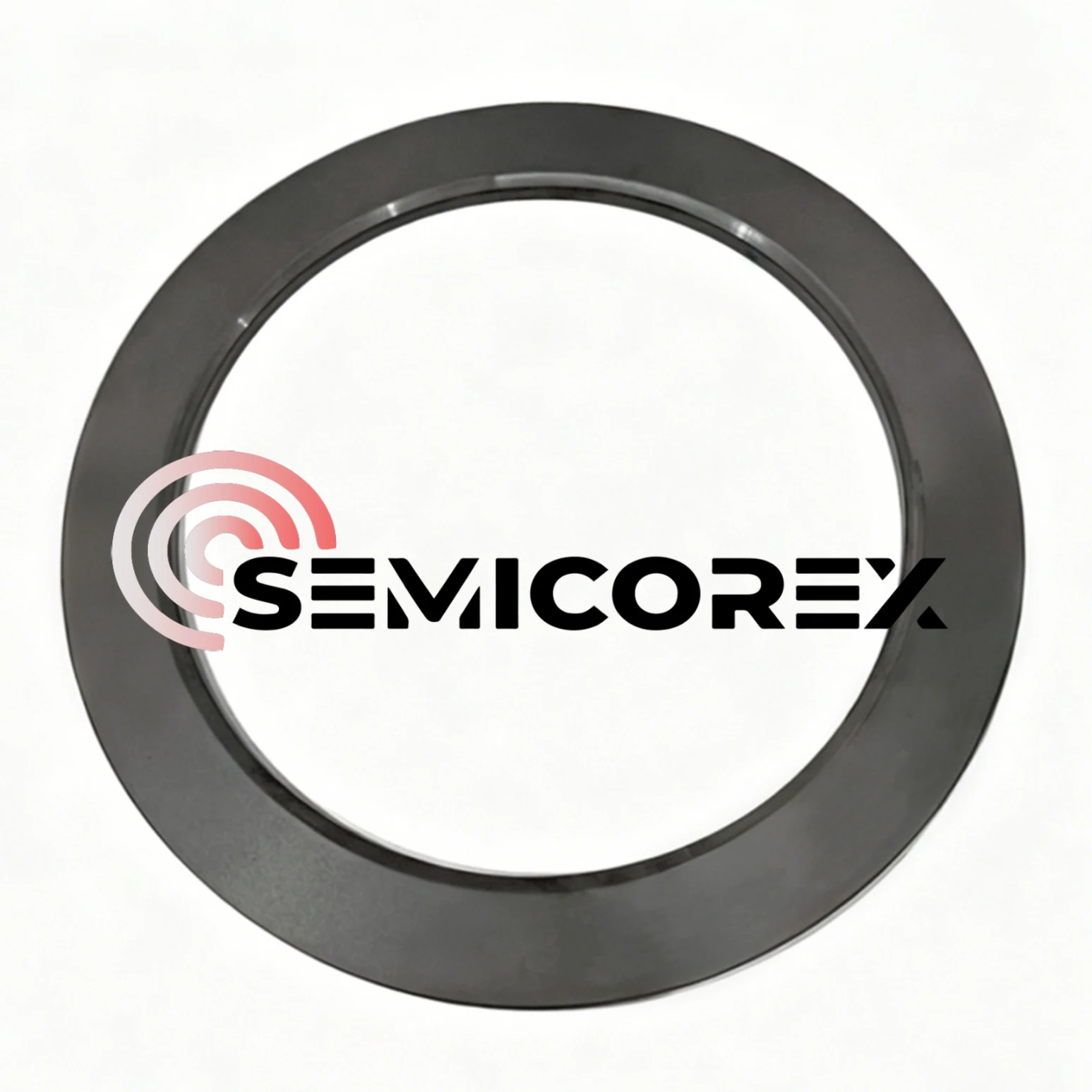
Keramische Fokusringe für Halbleiter
Semicorex-Keramik-Fokusringe für Halbleiter sind Hochleistungsringteile aus CVD-SiC-Materialien, die speziell für hochintensive Plasmaätzumgebungen entwickelt wurden. Semicorex ist ein branchenführender Hersteller von CVD-SiC-Keramik-Fokusringen für Halbleiter. Wir freuen uns auf Ihre Anfrage.
WeiterlesenAnfrage absenden
CVD-SiC-Fokusring für 2L10-506419-21
Der aus Hochleistungs-CVD-SiC-Materialien hergestellte Semicorex CVD-SiC-Fokusring für 2L10-506419-21 ist das entscheidende Ringteil, das speziell für TEL VIGUS RK4-Geräte entwickelt wurde, die in Präzisions-Halbleiterätzprozessen verwendet werden. Wenn Sie sich für Semicorex entscheiden, erhalten Sie die idealen CVD-SiC-Lösungen, um präzise und gleichmäßige Ätzergebnisse zu erzielen.
WeiterlesenAnfrage absenden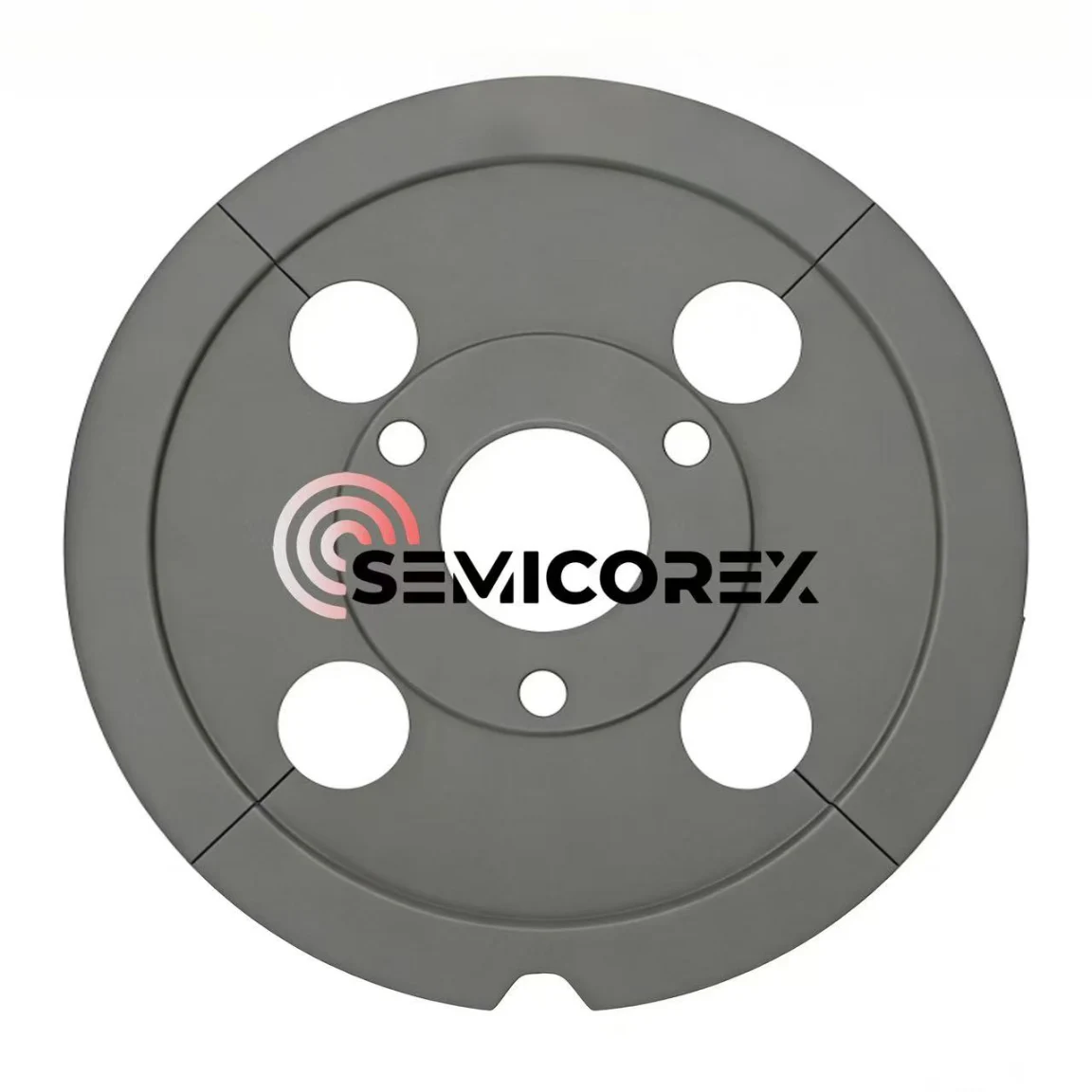
Massive Siliziumkarbid-Lamellen
Semicorex-Rippen aus massivem Siliziumkarbid sind hochleistungsfähige Komponenten, die präzisionsgefertigt aus massivem CVD-SiC hergestellt werden und hauptsächlich in Hochtemperaturöfen in Halbleiter-Wärmebehandlungsanlagen verwendet werden. Semicorex ist bestrebt, unseren geschätzten Kunden maßgeschneiderte Rippen aus massivem Siliziumkarbid in marktführender Qualität anzubieten und freut sich darauf, Ihr langfristiger Partner in China zu werden.
WeiterlesenAnfrage absenden
Semicorex produziert seit vielen Jahren CVD sic und ist einer der professionellen CVD sic Hersteller und Lieferanten in China. Sobald Sie unsere fortschrittlichen und langlebigen Produkte kaufen, die in Großpackungen geliefert werden, garantieren wir die große Menge in schneller Lieferung. Im Laufe der Jahre haben wir unseren Kunden einen maßgeschneiderten Service geboten. Kunden sind mit unseren Produkten und unserem exzellenten Service zufrieden. Wir freuen uns aufrichtig darauf, Ihr zuverlässiger langfristiger Geschäftspartner zu werden! Willkommen, um Produkte aus unserer Fabrik zu kaufen.