
- English
- Español
- Português
- русский
- Français
- 日本語
- Deutsch
- tiếng Việt
- Italiano
- Nederlands
- ภาษาไทย
- Polski
- 한국어
- Svenska
- magyar
- Malay
- বাংলা ভাষার
- Dansk
- Suomi
- हिन्दी
- Pilipino
- Türkçe
- Gaeilge
- العربية
- Indonesia
- Norsk
- تمل
- český
- ελληνικά
- український
- Javanese
- فارسی
- தமிழ்
- తెలుగు
- नेपाली
- Burmese
- български
- ລາວ
- Latine
- Қазақша
- Euskal
- Azərbaycan
- Slovenský jazyk
- Македонски
- Lietuvos
- Eesti Keel
- Română
- Slovenski
- मराठी
- Srpski језик
China CVD sic Hersteller, Lieferanten, Fabrik


- View as

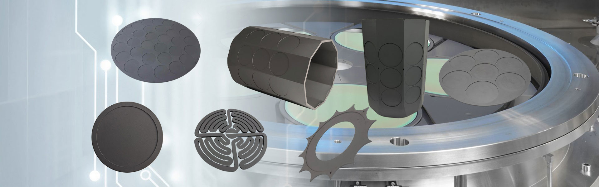
Massive CVD-SiC-Ringe
Die festen CVD-SiC-Ringe von Semicorex sind leistungsstarke ringförmige Komponenten, die hauptsächlich in den Reaktionskammern von Plasmaätzanlagen in der modernen Halbleiterindustrie verwendet werden. Die massiven CVD-SiC-Ringe von Semicorex unterliegen einer strengen Materialauswahl und Qualitätskontrolle und bieten beispiellose Materialreinheit, außergewöhnliche Plasmakorrosionsbeständigkeit und konstante Betriebsleistung.
WeiterlesenAnfrage absenden
Fokusringe aus Siliziumkarbid
Siliziumkarbid-Fokusringe, die entscheidenden Ringteile, wurden speziell entwickelt, um die Gleichmäßigkeit und Stabilität der Waferätzung beim Halbleiter-Plasmaätzen zu verbessern. Sie sind bekannt für ihre hervorragende Leistung bei der Förderung einer gleichmäßigen Plasmaverteilung und der Optimierung der elektrischen Feldumgebung.
WeiterlesenAnfrage absenden
CVD-SiC-Duschköpfe
Semicorex CVD-SiC-Duschköpfe sind hochreine, präzisionsgefertigte Komponenten, die für CCP- und ICP-Ätzsysteme in der modernen Halbleiterfertigung entwickelt wurden. Wenn Sie sich für Semicorex entscheiden, erhalten Sie zuverlässige Lösungen mit höchster Materialreinheit, Bearbeitungsgenauigkeit und Haltbarkeit für die anspruchsvollsten Plasmaprozesse.*
WeiterlesenAnfrage absenden
Randringe
Semikorex -Kantenringe werden von den führenden Halbleiter Fabs und OEMs weltweit vertrauen. Semicorex bietet Lösungen, die die Lebensdauer erweitern, Wafer-Gleichmäßigkeit optimieren und erweiterte Prozessknoten unterstützen.*
WeiterlesenAnfrage absenden
Gasverteilungsplatten
Semikorex -Gasverteilungsplatten aus CVD SIC sind eine kritische Komponente in Plasmaetchsystemen, die eine gleichmäßige Gasdispersion und eine konsistente Plasmaleistung über den Wafer gewährleisten. Semicorex ist die vertrauenswürdige Wahl für leistungsstarke Keramiklösungen und bietet unübertroffene materielle Reinheit, technische Präzision und zuverlässige Unterstützung, die auf die Anforderungen einer fortschrittlichen Semiconductor-Herstellung zugeschnitten sind.**
WeiterlesenAnfrage absenden
Solider SiC-Duschkopf
Der Duschkopf aus massivem SiC ist eine entscheidende Komponente in der Halbleiterfertigung und wurde speziell für chemische Gasphasenabscheidungsprozesse (CVD) entwickelt. Semicorex, ein führendes Unternehmen in der fortschrittlichen Materialtechnologie, bietet Duschköpfe aus massivem SiC an, die eine hervorragende Verteilung der Vorläufergase über Substratoberflächen gewährleisten. Diese Präzision ist entscheidend für die Erzielung qualitativ hochwertiger und konsistenter Verarbeitungsergebnisse.**
WeiterlesenAnfrage absenden
Semicorex produziert seit vielen Jahren CVD sic und ist einer der professionellen CVD sic Hersteller und Lieferanten in China. Sobald Sie unsere fortschrittlichen und langlebigen Produkte kaufen, die in Großpackungen geliefert werden, garantieren wir die große Menge in schneller Lieferung. Im Laufe der Jahre haben wir unseren Kunden einen maßgeschneiderten Service geboten. Kunden sind mit unseren Produkten und unserem exzellenten Service zufrieden. Wir freuen uns aufrichtig darauf, Ihr zuverlässiger langfristiger Geschäftspartner zu werden! Willkommen, um Produkte aus unserer Fabrik zu kaufen.